")
")
Research - Laboratory for Transport Measurements
Experimental setup in the Laboratory is adapted to transport measurements on thin semiconductor films. The transport measurements include:- Current – voltage (I – V) characteristics measurements for determination of the specific resistivity / conductivity of materials;
- Hall voltage measurements for determination of a sign and a concentration of charge carriers;
- Measurements of the time dependence of photocurrent for monitoring slow dynamics of photoexcitations in materials.
The material to which we dedicate a great part of our research is zinc oxide (ZnO) in a form of thin films of thicknesses between 10 nm and 100 nm, synthesised by a method of atomic layer deposition (ALD). ZnO is a wide gap semiconductor with an energy gap of 3.2 – 3.4 eV. A property, which distinguish ZnO from other metal-oxide semiconductors, is a capacity for high concentrations of point defects (vacancies, interstitials) in the crystal structure. Those defects determine in a high degree physical properties of ZnO. For example, values for ZnO specific resistivity can span six orders of magnitude – from 10-3 Ω cm to 103 Ω cm, depending on the defect concentration. By changing parameters of the ALD synthesis, we can obtain ZnO thin films with different physical properties. Transport measurements can give us valuable information about the synthesised materials, which we use in further research that is oriented towards applications of ZnO in fields of photocatalysis and photovoltaics.
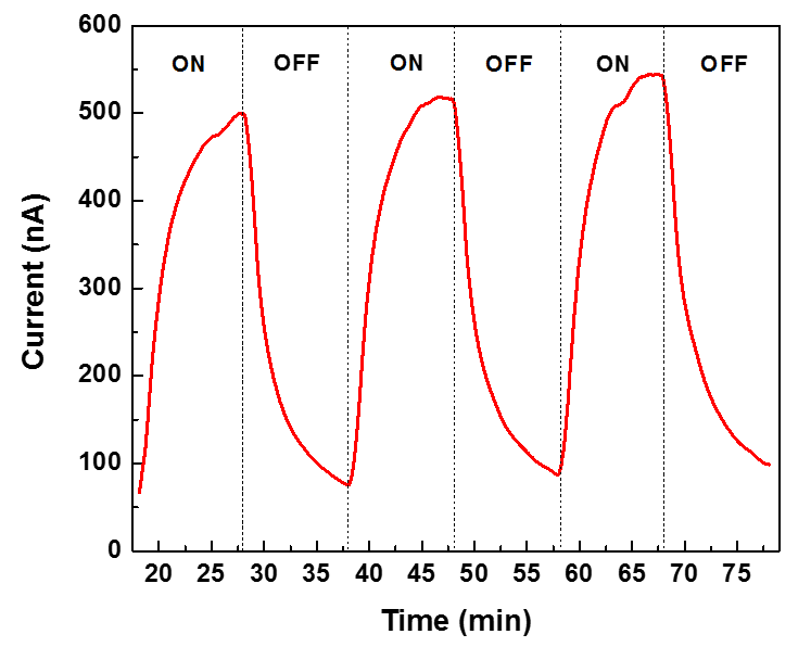
Figure: Time response of photocurrent in thin ZnO film on UV photoexcitation.
Contact
FACULTY OF PHYSICS
UNIVERSITY OF RIJEKA
Ulica Radmile Matejčić 2
51000 Rijeka
Tel.: +385 51 584 600
Fax: +385 51 584 649
Email: fizika@phy.uniri.hr
 |
 |
|
|
|
 |
 |
 |
|
 |
|
|
|
|
 |
|
 |
|
 |
|
 |
|
 |
 |